Before we dig into the details of this paper, let’s cover some important information you’ll need to understand.
Feeling a bit lost? This article is the first part in a series on the paper “Charlib: An Open Source Standard Cell Library Characterizer”. If you’re looking for the other parts, or the paper itself, click here.
Some Assumptions
I'm aware of the risk I'm taking here. | xkcd.com/1339
I’m going to assume that you, an intellectual, have some knowledge going into this. Probably a big part of why you clicked on this article, right?
- You should know how to read a line graph
- You should have at least a basic understanding of Boolean algebra
- You should be able to identify the components of a circuit diagram (including logic gates) and know how they work on a basic level
- You should be aware of hardware descriptons languages (aka HDL) such as verilog or VHDL (but don’t worry, we won’t be working with any code here)
There’s a lot of technical stuff listed there, but don’t be intimidated. Even if you aren’t super familiar with some of these concepts, I’d encourage you to read on anyways. If you find yourself getting confused, take a step back and review. I’ve tried to provide helpful links up above. As always, if you have questions you can send me an email.
Now that that’s out of the way…
Let’s start with a bit of background
Even if you’ve studied electronics at a university level, odds are pretty good that this is your first time hearing the term “standard cell”, let alone paired with “library” and “characterizer”. We’ll begin by breaking down what those terms mean.
What are Standard Cells?
In the simplest terms, standard cells are digital building blocks implemented in a consistent, standardized way. They’re the same logic gates you know and love, just a bit more… standard.
Perhaps an analogy will explain this a little better.
Imagine you’re building a house. You’ve got the framing up and the roof on, and now it’s time to cover up the exterior walls with siding. You can hire an expert stonemason who will build you a beautiful natural stone veneer, but the job will take a month, and they charge expensive rates for their expertise. Or instead, you can hire a bricklayer who will have the job done by the end of the week for a fraction of the cost.
See the difference here? The stonemason has to work with the shapes of the stone he or she is given. The bricklayer doesn’t have to worry about that at all - all the bricks have the same dimensions, so it doesn’t matter that brick A is next to brick C instead of brick B. As a result, the brickwork is quick and cheap by comparison, and the bricklayer doesn’t have to be a master of his craft (though it certainly helps).
It’s the same way with electronics. Standard cells (like bricks) have a fixed height, so we can place them in rows (like bricks) to get a clean, organized design. A master engineer (like the stonemason) could likely do a better job without those rows, but it would probably take them so long that it isn’t worth the cost and effort.
I don't see a difference here. | cell image from vlsitechnology.org
If that analogy didn’t make sense to you, maybe this way of thinking about it will. Think of standard cells like Lego bricks: they all have the same height, and they connect in predictable ways. They aren’t all exactly the same shape. Some are wider than others and some are narrower. On their own they aren’t very special. But put a bunch of them together, and you can create something much more interesting.
When using standard cells, we don’t have to think about physical design problems, such as how transistor M1 connects to to transistor M3 with wires that are a few nanometers wide. Instead we get the luxury of abstraction: we can just think about how the logic works. This seriously reduces the amount of work involved in implementing a design, and has saved this engineer many headaches.
There are a lot of other problems that standard cells solve for us, but we won’t go into that here. That’s a topic for another post.
Ok, but what does a Library have to do with it?
A standard cell library is a collection of standard cells that are made to work well together. They’ll all have the same height, and you’ll have cells for all the major logic components: AND, OR, XOR, NAND, et cetera. You’ll also have things like inverters, buffers, and flip-flops. Think of a standard cell library like a toolbox full of devices for working with digital logic.
Seems pretty straightforward, right? But consider how powerful this idea is! With a standard cell library, I can take any digital logic design and turn it into a real physical design. We even have automated software tools to do this. You hand the tool a standard cell library and some HDL, and the tool “synthesizes” your design using the cells in the standard cell library.
If you’re working with a standard cell library, you’ve probably come across the term “process design kit” (or PDK for short). A PDK is a larger set of documents, tools, and design data relavant to a particular semiconductor manufacturing process. For an example, check out this open source PDK based on SkyWater’s 130nm process.
Don’t get confused: a standard cell library is not the same thing as a PDK. Usually a PDK will contain a standard cell library, but it’s just a small part of a much bigger collection of tools. However, you may occasionally see standard cell libraries referred to as “cell kits”.
There’s a little more to synthesis than just replacing all the &’s in your HDL with cell names, of course. A good synthesizer considers the electrical properties of cells and makes tweaks to your design to ensure everything will work right. Different synthesizers do this differently, but they all have one thing in common: they have to know the properties of every standard cell in the library.
How do we determine the electrical properties of standard cells in a library? Through characterization.
Standard Cell Library Characterization
Characterization is the process of determining the characteristics of something. This doesn’t just apply to electronics, of course. You can characterize all sorts of things in all sorts of ways. I can characterize an apple as sweet and crisp. Or I could characterize an Apple as a thin and light laptop with a retina screen and an M3 processor.
But in the context of standard cells, we want very specific information. Standard cell characterization is the process of measuring how a cell shapes signals.
Let’s pause and unpack that a bit. What do we mean when we talk about shaping input signals?
A simple example
Consider the simplest cell: a 1-bit buffer. It has a single input and a single output. If you feed in a logical 1, it will spit out a logical 1 and likewise for logical 0. Its whole job is to give you the exact same value you put into it.
A buffer gate and its truth table. | allaboutcircuits.com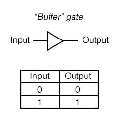
Now let’s say I connect the input of a buffer to a signal generator, connect the output to a small capacitor, and feed in a signal that slews from 0 to 1 over a very short amount of time, like this:
Let's see how that buffer handles this! (cue maniacal laughter)
We can expect the output to look exactly the same, right? Well, almost. Reality is a bit more complicated than that. Take a look at the simulation results below.
For completeness: these plots are generated using CharLib with the standard cells in the open source gf180mcu_osu_sc PDK.
Look at all that delay. Reality is a bummer sometimes.
As it turns out, the buffer introduces a little bit of delay to the signal; it takes time for the change in the input signal to “propagate” through to the output signal. This is called the “propagation delay”, or \(t_{prop}\) for short.
It also takes a little longer for the output signal to transition from 0 to 1 than the input signal does. This is called the “transient delay”, or \(t_{trans}\).
This is more or less what you'd see if you connected an oscilloscope to a circuit like this.
Both of these values change depending on the structure of the standard cell we’re testing, the amount of capacitance we connect to the output (\(c_{load}\)), and the amount of time we give the input signal to slew (\(t_{slew}\)), among many other factors.
For combinational cells (logic gates, buffers, inverters… pretty much anything that doesn’t require a clock input for sequencing), these two delay characteristics provide a pretty good model of how the cell will respond to input.
But what if we feed in an input signal that transitions faster or slower? Or what if we put a larger capacitor on the output, so that the cell has to do more work in order to charge it to a logical 1?
Changing conditions
If we want to have a good model of how our buffer shapes signals, we need to take measurements under a bunch of different conditions. So we change the test configuration by adjusting the parameters listed below (at minimum):
- \(t_{slew}\), the amount of time the input signal takes to “slew” or transition from 0 to 1. This is also known as the slew rate. It’s usually measured in nanoseconds or picoseconds.
- \(c_{load}\), the total capacitance the cell has to drive on the output. This is also called “fanout” (for reasons we’ll get into later), and is usually measured in picofarads or femtofarads.
This is where things start to get complicated. We want to see how varying both of these conditions at the same time affect the cell’s \(t_{prop}\) and \(t_{trans}\). So, for every value of \(c_{load}\) we want to test, we have to simulate with every value of \(t_{slew}\). This results in a 3-dimensional surface of data for each delay value we want to measure. Our test conditions are shown along the x and y axes, and the delay is plotted on the z-axis.
This chart shows how both types of delay are affected by varying our test conditions. Pretty neat, huh?
This isn’t as easy as it sounds
Everything we’ve discussed so far has been in the context of the humble buffer. Like platypuses (platypi? platypeople?), they don’t do much. The moment we start talking about anything more complicated, we have problems to solve.
For example, consider a simple 2-input AND gate. It’s not a complicated device, by any stretch of the imagination. But since it has 2 inputs, we have to deal with some additional complexities:
- There are now multiple paths through the gate (one path from each input to the output), and each may shape signals in different ways.
- If we’re testing the path from input A to the output, we have to make sure input B has a logical 1 (otherwise it would “mask” the signal, and we would never see it propagate through to the output). We call this the “nonmasking condition” for input B.
This is still just a simple gate, of course. Sequential devices, such as latches and flip-flops, add a boatload of extra problems:
- We now have to stimulate the cell with a clock signal that has an appropriate period and slew rate, in addition to stimulating the inputs.
- Not only do we have to deal with multiple inputs, but we also have to make sure we measure the correct state transition. The more states a cell has, the more complex this is.
- Since we don’t know what state the cell will be in after initilization, we have to develop procedures to reset each device to a known state before testing anything, then perform this reset procedure for every test we run.
- Memory devices have specific timing requirements:
- Inputs have to be held stable for a particular amount of time before the clock edge. This is called the setup time, or \(t_{setup}\).
- Inputs also have to be held stable for some amount of time after the clock edge. This is the hold time, \(t_{hold}\).
- \(t_{setup}\) and \(t_{hold}\) have an interdependent relationship, as explored by Salman et. al. So adjusting one might affect the other, and vice versa.
Clearly complexity scales up, fast. Any additional factor we add, like an extra input or internal state, may double or even triple the amount of work we have to do to characterize a cell. And we have whole libraries of them to deal with! Yuck!
Is it even worth it?
Gee, this sure sounds like a lot of work to do just to measure some timings. Wouldn’t it be better
if we just, y’know, didn’t do all this characterization stuff? Unfortunately for lazy efficient
engineers like you and me, there are good reasons behind the standard cell characterization
process. It all comes down to the need for faster logic.
If you’ve ever looked into how a computer works, you know that a processor runs at a certain clock speed. Each time the clock ticks, the processor executes one instruction; that is, it completes one small task, such as adding two numbers or storing something for later use. The speed of a processor (or any logic design) is limited by the amount of time it takes to complete one instruction; if the clock ticks before execution is done, data can be lost. This limiting factor is usually the slowest physical path through the processor’s execution unit, and is called the critical path.
This is a HUGE oversimplification of how a processor works. If you’re interested in learing more, I recommend David Harris and Sarah Harris’s textbook Digital Design and Computer Architecture. I’ve linked the RISC-V Edition, but there are other editions out there for other architectures like ARM and MIPS.
So as logic designers, if we want faster execution we must be aware of the critical path in our designs. We could perform transistor-level simulation after every single change we make to a design, but this is really slow and gives more detail than we actually need most of the time. We usually just want to know if we have any chance of meeting timing specifications. With characterized standard cells, we can quickly and easily identify the critical path in a design because we know how much delay each cell introduces, and how much each cell stretches out an input signal. We can start with the specifications of our input signals, step through each level of logic in our design, and end up with a pretty good estimate of how much time it takes that signal to propagate to the output. This is called static timing analysis or STA.
The big advantage of STA is that it takes a miniscule fraction of the time that it takes to run transistor-level simulation. This means that we can iterate on designs much faster, and only run detailed simulation when we’re pretty confident our design is ready to be manufactured. This saves a ton of compute cycles, making characterization very worthwhile.
Putting it all together: Static Timing Analysis
Suppose you have a small design like the one pictured below. Nothing too complicated. You just want to know whether it will meet your timing requirements.
Yeah, this design doesn't do anything helpful.
See how we have the output of one gate driving the inputs to several other gates? Each of those gates has a very small amount of input capacitance. They don’t have much on their own, but when they connect in parallel like this it can become significant. Together they act a lot like one larger capacitor on the output of the driving gate. Does that sound familiar? Perhaps you can guess where we’re headed.
Recall how we took our characterization measurements: we fed in a signal with a known slew rate, then measured the delay associated with charging a load capacitor. Now we’re going to use those measurements to estimate delay.
The best part is we get to ignore 90% of the circuit.
First we zoom in on a single cell. Since we know the input capacitace of the cells it’s driving, and all those cells are wired in parallel, we can add up those capacitances and model them as a single larger capacitor. Presumably our signal generator will also have some slew rate limit, so we can use that spec as our input slew rate. Since we now know \(c_{load}\) and \(t_{slew}\), we can look up the delays from the characterization data for this cell. We keep a tally of the total propagation delay, and use the transient delay as the input for the next logic layer.
We repeat this process for each layer of logic in our design, keeping track of delays and how they affect the signal feeding into the next layer. By the time we get to the output, we know exactly how long our critical path is. Hooray for STA!
Conclusion
We’ve covered a lot of information here. If you’re still with me, give your brain a minute to digest all of that.
Take some time to review what you need. When you feel prepared, move on to part 2. There we’ll go into detail on the characterization process.